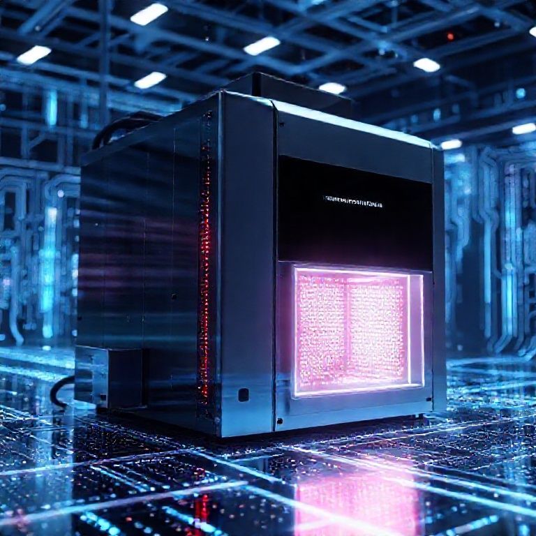
ACM’s Ultra Lith BK: A New Dawn for Lithography Precision
ACM Research has unveiled its Ultra Lith Baker (Ultra Lith BK), a cutting-edge system designed to revolutionize advanced lithography. The first unit has already been delivered to a major global display panel manufacturer, signaling a significant step forward in addressing industry-wide challenges related to process uniformity and thermal drift. This innovation promises to enhance the stability and repeatability of lithography processes, crucial as device geometries shrink.
The Ultra Lith BK tackles critical issues like process non-uniformity and CD variation head-on. Its UV curing system boasts an impressive ±5% UV intensity uniformity, ensuring consistent resist hardening across the wafer. The system’s versatility is further enhanced by supporting line-scan, rotary, and hybrid UV-curing exposure modes, offering maximum process flexibility to meet diverse manufacturing needs.
The implications of the Ultra Lith BK extend beyond just display panel manufacturing. Its advanced thermal management architecture significantly reduces CD variation, overlay error, and pattern distortion. These improvements are vital for boosting yield and ensuring long-term process reliability in semiconductor manufacturing, where precision is paramount for creating increasingly complex and miniaturized devices.
According to Dr. David Wang, President and CEO of ACM, maintaining uniform process control is essential for consistent yield and device performance as lithography pushes the limits of precision. The Ultra Lith BK’s deployment represents a key milestone for ACM’s Track series and marks its entry into the display panel market, a sector known for its high-volume production and stringent equipment performance demands.
The Ultra Lith BK’s combination of high uniformity, configurable architecture, and multiple exposure modes positions it as a game-changer. By minimizing variability and enabling scalable production, it empowers manufacturers to confidently navigate future technology nodes. This innovation promises to be a key enabler for advancements in both display and semiconductor technologies.

